In a scanning electron microscope (SEM) a focused electron beam is scanned over the sample. The electrons interact with the material which produces secondary quantities or backscatters the electrons themselves. Among the first are secondary electrons (SE), characteristic X-rays, or light (cathodoluminescence, CL).
Secondary electrons stem from the top few nanometers of the sample and therefore provide strong topographic information. Characteristic X-rays are formed by the excitation of inner-core shell electrons and provide element-specific data via energy-dispersive X-ray spectroscopy (EDX). In CL electrons from the valence band are excited into the conduction band. When the material relaxes into the ground state photons in and close to the visible range are emitted which reveal corresponding local optical properties. Elastically backscattered electrons (BSE) can be either used to visualize mass-density variations in the material or, when recorded with a 2D detector, provide crystallographic information (via electron backscatter diffraction, EBSD). Please check below for the corresponding equipment of the SEMs in the facility.
The achievable spatial resolution depends on the electron energy and current but is ultimately limited by the interaction volume of the electrons with the material and the depth from which the secondary signals can escape. SE microscopy provides the highest spatial resolution with approximately 1 nm for low beam energies. For all other techniques, the interaction volumes are bigger and therefore resolution is reduced.
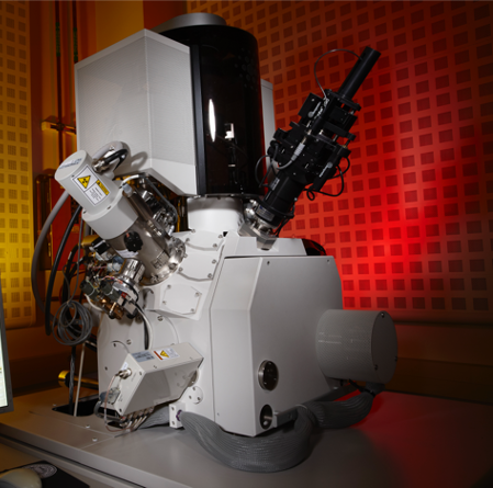
FEI Helios Dual-beam 600 FIB/SEM
A high-resolution dual-beam focused ion beam and scanning electron microscope. The instrument is equipped with an Elstar field emission SEM for nanometer resolution imaging and a Tomahawk FIB column operating from 30 kV down to 500 V. Ion currents range from 7 pA, providing a minimal beam size of 7 nm, to 22 nA which can be used for substantial milling tasks. The very stable piezo-driven stage can operate on an area of 150 x 150 mm. Attached is currently a gas source for platinum deposition as well as an Omniprobe manipulator that is typically used for the transfer of TEM and APT samples.
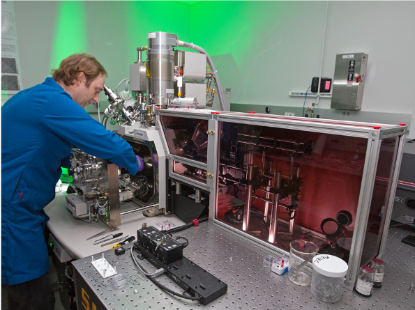
Tri-Beam Laser/FIB/SEM
Dual-beam focused ion beam and scanning electron microscope equipped with a femtosecond laser and associated scanning and focusing optics. The laser can be used for automated serial sectioning of volumes up to 1 mm³, combined with multimodal imaging and spectroscopy using SEM, electron backscatter diffraction (EBSD), and energy dispersive spectroscopy (EDS). The electron column and detectors are optimized for high-current operation at up to 400 nA, which enables rapid EBSD and EDS acquisition for 3D characterization.
FEI Nova Nano 650 SEM
High-resolution scanning electron microscope; equipped with a high stability Schottky field emission gun and a large specimen chamber (379 x 280 mm door size); Voltage: 500-30 keV; Resolution: 1.2 nm @ 30 keV. Detectors include an ETD detector for basic secondary electron imaging and a through-lens detector for high-resolution SE imaging. Backscattering detector for Z-imaging.
Thermo Scientific Apreo C LoVac SEM
High-resolution scanning electron microscope; equipped with a high stability Schottky field emission gun and a large specimen chamber (340 mm chamber diameter); Voltage: 100 eV - 30 keV; Resolution: 0.8 nm @ 30 keV, 1.3 nm @ 1 keV; LoVac capable up to 500 Pa chamber pressure. Detectors include standard SE; dedicated backscattering detector for Z-imaging; T1 and T2 through-lens detectors for high-resolution imaging; LoVac SE detector; LoVac backscatter detector; EDAX Si-drift EDX detector for highly efficient recording of elemental maps; EDAX EBSD detector for crystallographic analysis; cathodoluminescence (CL) detector for optically active materials; EBIC amplifier for analysis of defects in semiconductors.
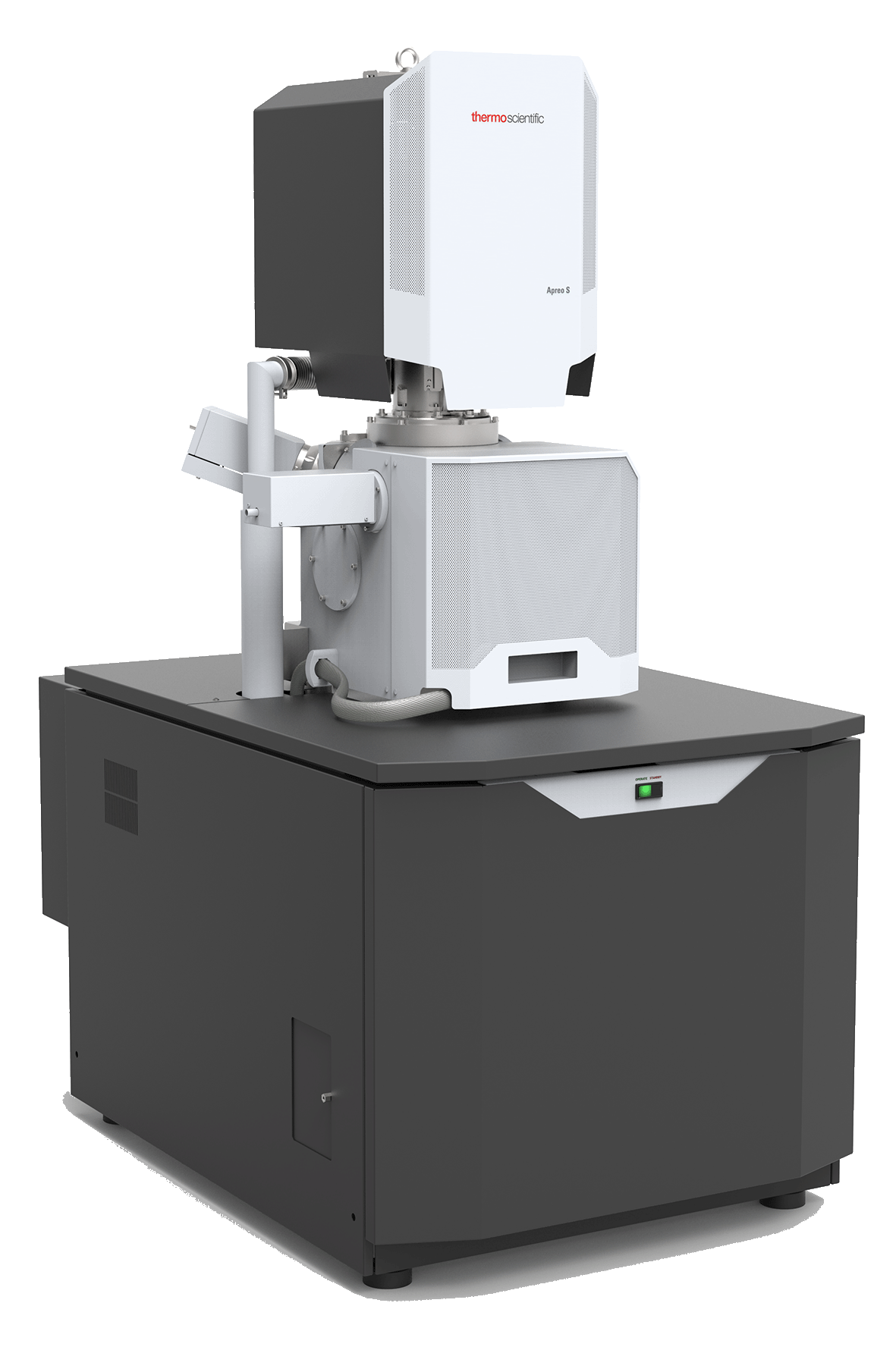
Thermo Scientific Apreo S SEM
High-resolution scanning electron microscope; equipped with a high-stability Schottky field emission gun and a large specimen chamber and compound electrostatic/electromagnetic immersion lenses. Detectors include standard SE; dedicated backscattering detector for Z-imaging; T1, T2, and T3 through-lens detectors for high-resolution imaging; STEM detector; direct electron detector (SEMCAM) with adjustable degrees of freedom for electron backscattered diffraction or transmission geometries.