A beam of electrons is transmitted through an ultra-thin specimen where the electrons interact with the material. The sample can be either illuminated with a focused beam that is scanned over a region (STEM) or with a broader beam of parallel electrons (TEM). Samples have thicknesses ranging from a couple of hundred down to a few nanometers. The latter allows visualizing the atomic structure of the material. The typical energy range of the primary electrons lies between 80 and 300 keV. Due to the high energies and corresponding small wavelengths of the electron wave, the achievable spatial resolution is in the Angstrom range.
The primary mode of interaction is the elastic scattering of electrons which leads to material-specific diffraction. The microscope's imaging objective lens can visualize the diffracted signal directly in its focal plane or construct an image in its image plane. The corresponding signal is further magnified by projector lenses and then detected by electron-sensitive detectors, in the case of STEM typically by an annular ring detector with the microscope set in diffraction mode, in the case of TEM the image is recorded with help of a CCD camera.
Additionally, the electron can transfer characteristic energies to the sample by exciting inner degrees of freedom. For TEM relevant excitations are phonons, plasmons, and characteristic X-rays. Those energy losses can be analyzed via electron energy loss spectroscopy (EELS). Characteristic X-rays are detected with an energy-dispersive X-ray spectrometer (EDX). Overall, TEM and STEM provide a versatile and powerful set of tools that allow the exploration of materials morphology, chemistry, and crystallography on the nanometer scale down to the atomic level.
Traditional TEM analysis is based on the premise that the sample is thin enough to capture a quasi-two-dimensional representation of the material. Nevertheless, many material systems contain complex three-dimensional morphologies with characteristic lengths of a few nanometers. The microscopy facility is equipped with dedicated sample holders and computational capabilities to record tilt series and reconstruct corresponding 3D electron tomograms.
The first crucial step for a successful TEM analysis is the preparation of a high-quality sample with the right thickness whereas the procedure is typically material specific. The microscopy facility provides all necessary tools in form of FIB, ion mills, and dedicated polishing equipment.
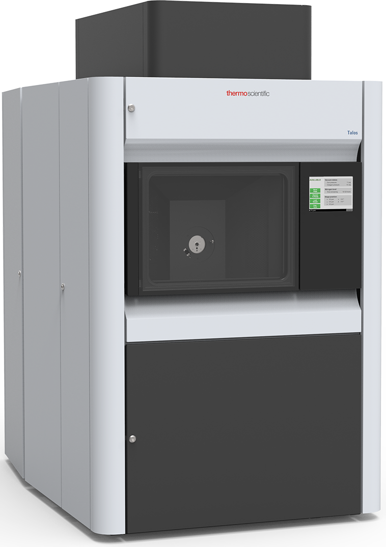
Thermo Scientific Talos F200X
This instrument is a scanning transmission electron microscope (S/TEM) equipped with a high brightness and high electron beam current (up to 50 nA) XFEG field emission gun and a symmetrically arranged quadrant XEDS detector system delivering high resolution and high throughput 2D/3D S/TEM imaging and chemical mapping. Owing to its high brightness electron gun configuration, Talos F200X provides better than 0.1 nm HRTEM line resolution and 0.16 nm STEM resolution. The system is also equipped with a direct electron detector for low-dose TEM experiments. Additionally, an integrated free scan module coupled with the direct electron detector allows for 4DSTEM acquisitions.
Features
- XFEG Schottky Field Emission Gun
- 200 kV to 80 kV Accelerating Voltage
- TEM and STEM Imaging Modes
- Super-X SDD XEDS detector (0.9 sr)
- BF/DF2/DF4 (four segmented)/HAADF STEM detectors
- CETA M16 plus Camera Speed Enhancement (30 fps at 4kx4k pixel resolution)
- Direct Electron Detector (DE-16, DE-FREESCAN)
- 3D S/TEM and EDS tomography
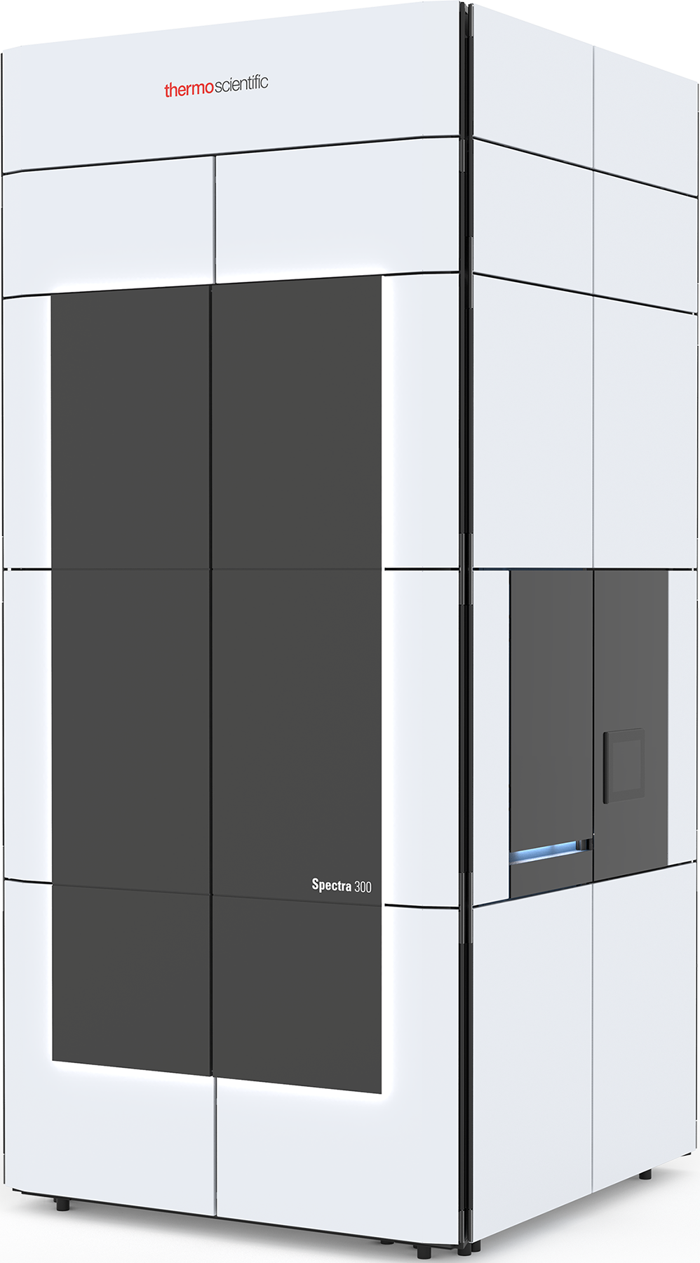
Thermo Scientific Spectra 200
This instrument is a probe aberration corrected (S-CORR) S/TEM equipped with a cold field emission gun (X-CFEG). The combination of high brightness X-CFEG and 5th order aberration corrector S-CORR delivers ultimate sub-Angstrom STEM image resolution at the accelerating voltages of 60 kV to 200 kV. The Spectra 200 contains Thermo Scientific symmetric quadrant XEDS detector configuration, achieving fast conventional and atomic resolution chemical mapping as well as 3D XEDS tomography. The system is also equipped with a 16-segment Thermo Scientific Panther detector system enabling improved differential phase contrast (DPC) and integrated differential phase contrast (iDPC) imaging in STEM.
Features
- X-CFEG Cold Field Emission Gun
- SCORR 5th order probe aberration corrector
- 200 kV to 30 kV Accelerating Voltage
- Panther STEM detectors
- Super-X SDD XEDS detectors (0.7 sr)
- CETA-S TEM Camera